The previous post ended with a promise: two TDA7294s on perfboard, a 13.8 → 52 V boost module, a dummy load — and then the motor gets to vote. The signal side was proven; the power side was still a pile of parts.
This post is about the two days I spent bringing up the first of those two amplifier channels, and about a 2 V notch in the top of a sine wave that took four hypotheses to kill.
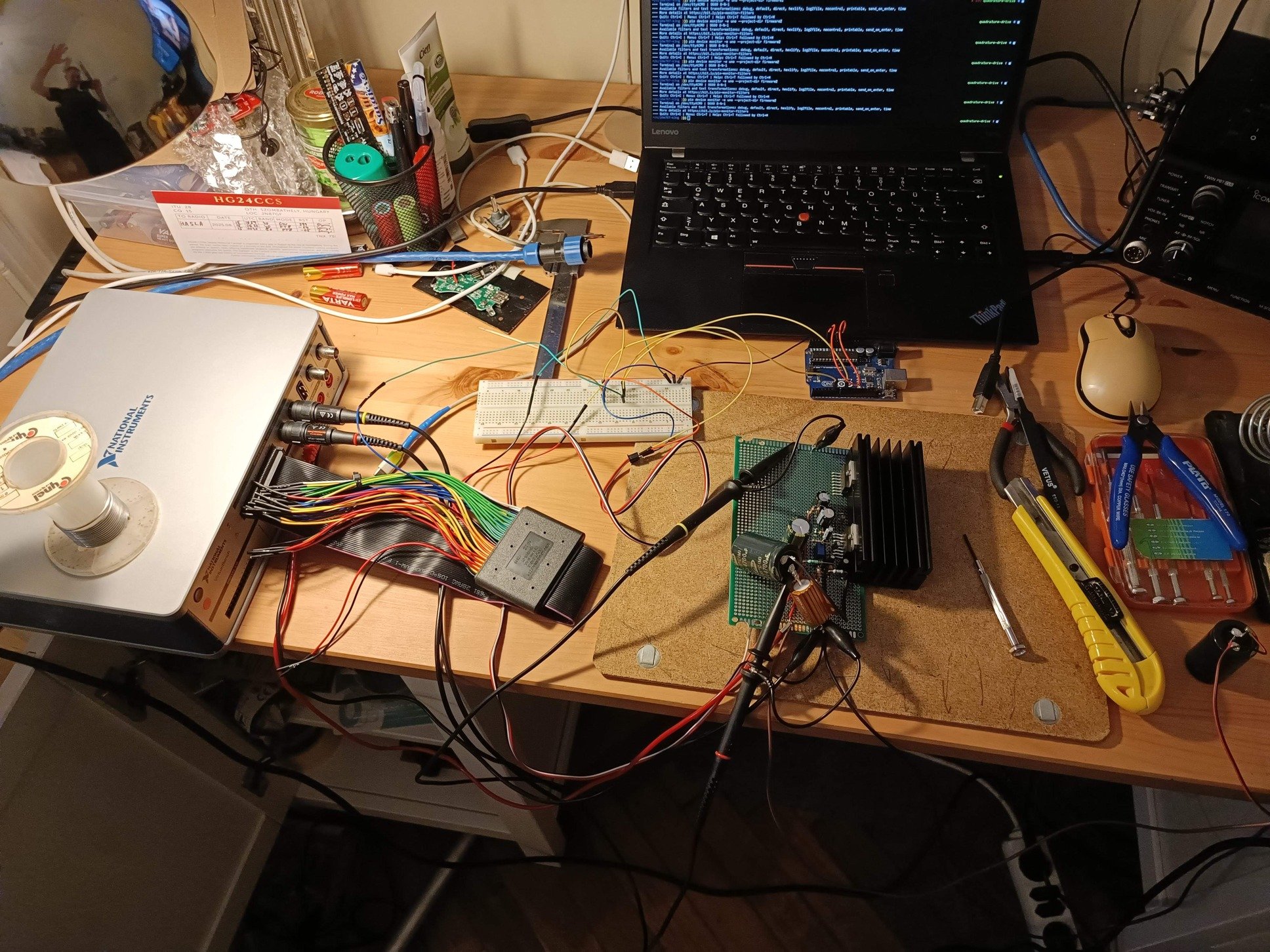
The amplifier
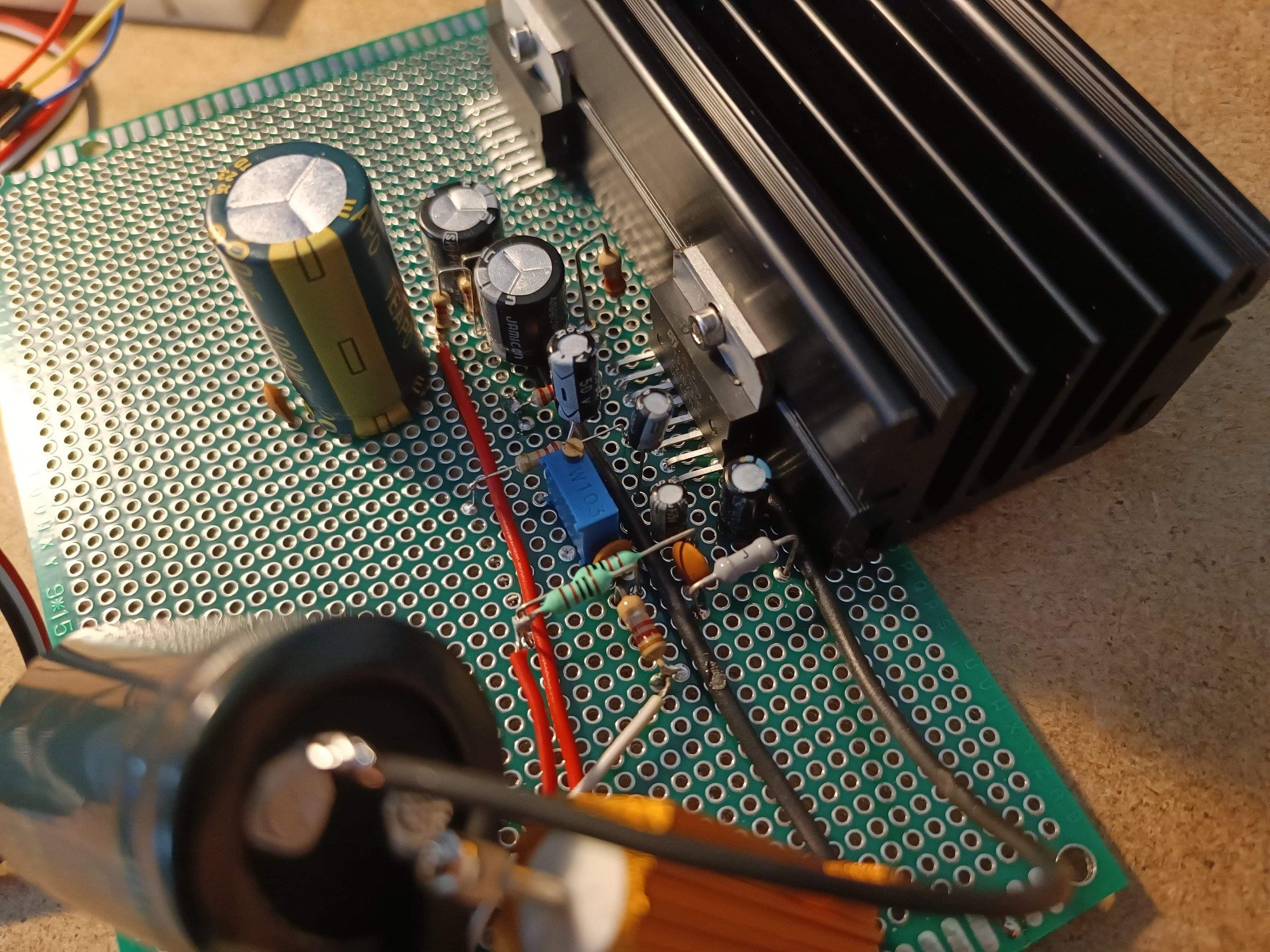
The TDA7294 is an audio chip, and this is emphatically not audio. Single supply, 52 V, so the output sits at 26 V and swings around it, with a 4700 µF capacitor coupling it into the winding. Gain is 1 + 22k/1.2k ≈ 19.3. MUTE and STBY are driven together from one Arduino pin, so the amplifier stays silent through MCU reset.
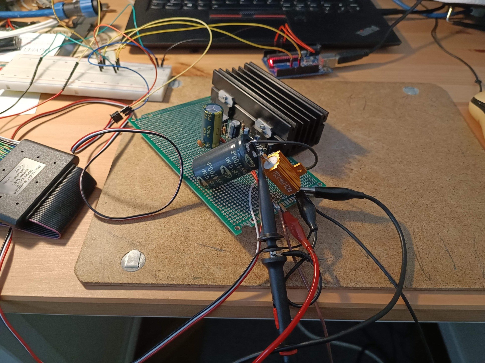
The load for all of this was a single 22 Ω 25 W power resistor — I bought two, one per channel. 22 Ω is about what a winding looks like at 60 Hz, and at full output it dissipates 14 W and gets genuinely frightening.
30 V: everything is fine
First light at a 30 V rail, and the result was better than it had any right to be: a 14.43 V peak sine, 10.2 V RMS, deviating from a perfect sine by 0.56 %. The flat region at the peak matched an ideal sine’s to within 2 %, positive and negative alike.
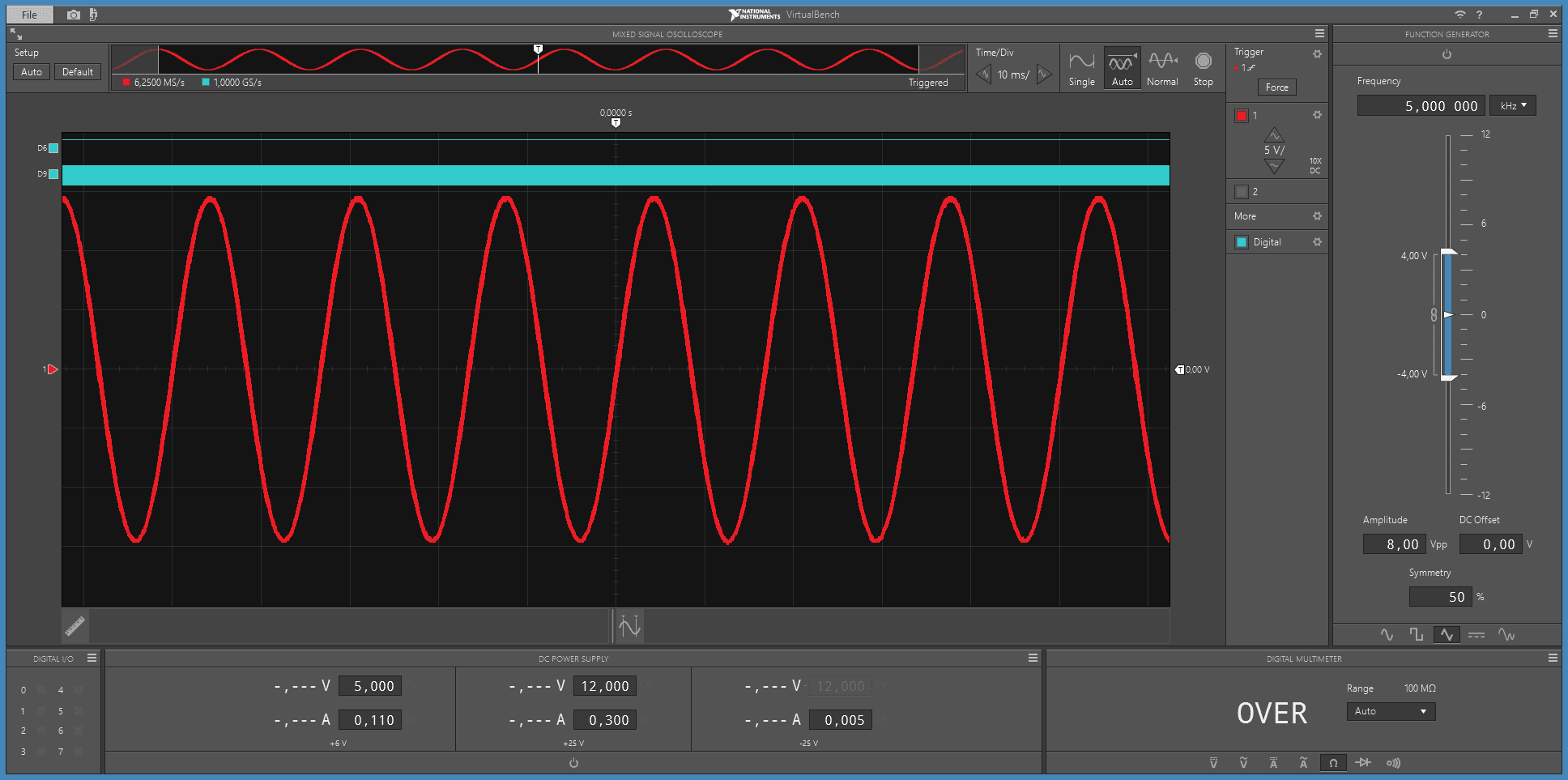
One number from that screenshot matters much later, so remember it: at 30 V the amplifier swung to within 0.6 V of its supply rail.
52 V: a notch appears
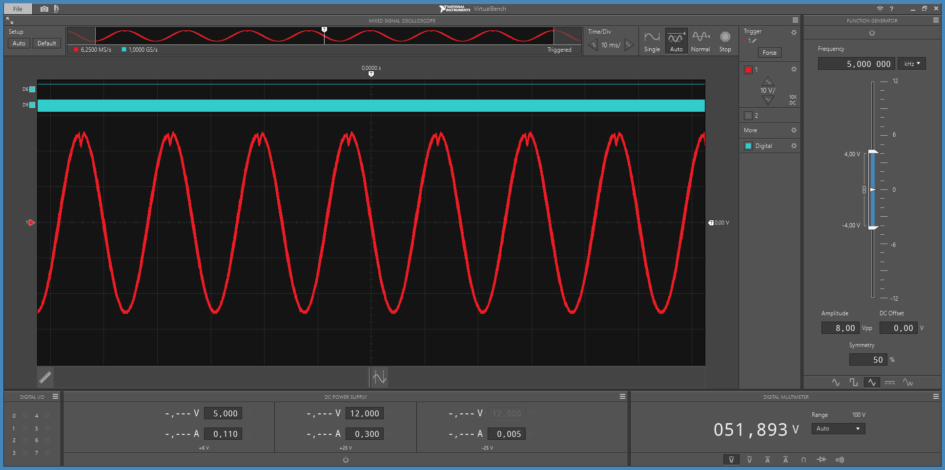
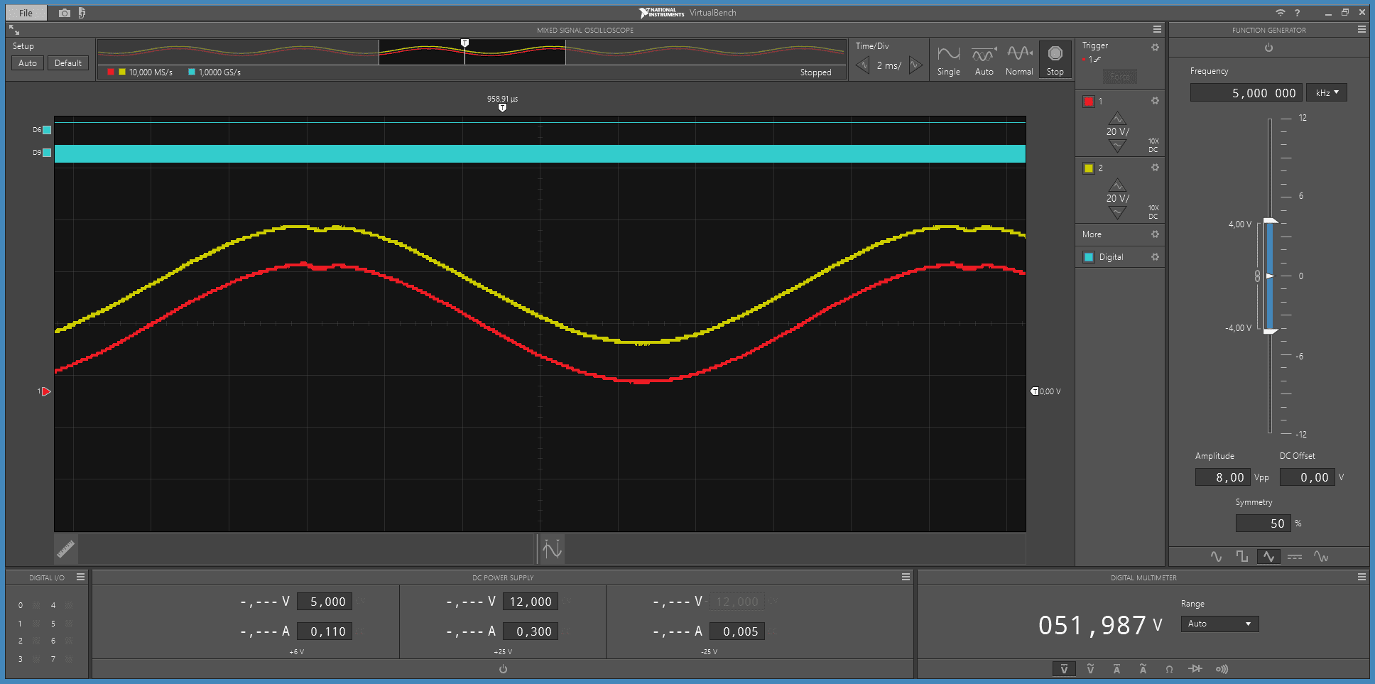
Rail up to 52 V, trimmer up to the design point of 17.7 V RMS, and the top of every cycle grew a sharp V-shaped notch, about 2 V deep and 0.5 ms wide, whose second horn was higher than its first. Deviation from a sine went to 1.9 %.
Four suspects, in the order I chased them.
Suspect 1: the bootstrap capacitor
The TDA7294 has a bootstrap pin that supplies the high-side driver from a 22 µF capacitor referenced to the output. If that capacitor sags while the output sits near the rail for 8 ms, the top device loses drive, the output dips, the dip recharges the capacitor, and the output recovers — which is exactly the shape I was looking at.
It was plausible on design grounds too. This project deliberately scaled its coupling capacitors for 5 Hz rather than audio, but left the bootstrap at the datasheet’s audio value of 22 µF.
Killing it took one measurement: probe pin 6 and pin 14 on separate channels, both DC coupled at the same scale, and read the gap between the traces.
| Phase | pin 6 − pin 14 |
|---|---|
| At the crest | 14.75 V |
| Mid-rise | 15.05 V |
| At the trough | 14.96 V |
Flat to within one pixel of the graticule. Not the bootstrap.
A warning if you try this: probe to ground, never with a probe’s ground clip on pin 14. All the scope grounds are common, so that clip would short the amplifier’s output through the probe leads.
Suspect 2: the PWM carrier
While zoomed in, a different problem showed up: a 62.5 kHz sawtooth riding on the output, 2.96 V p-p on the slopes.
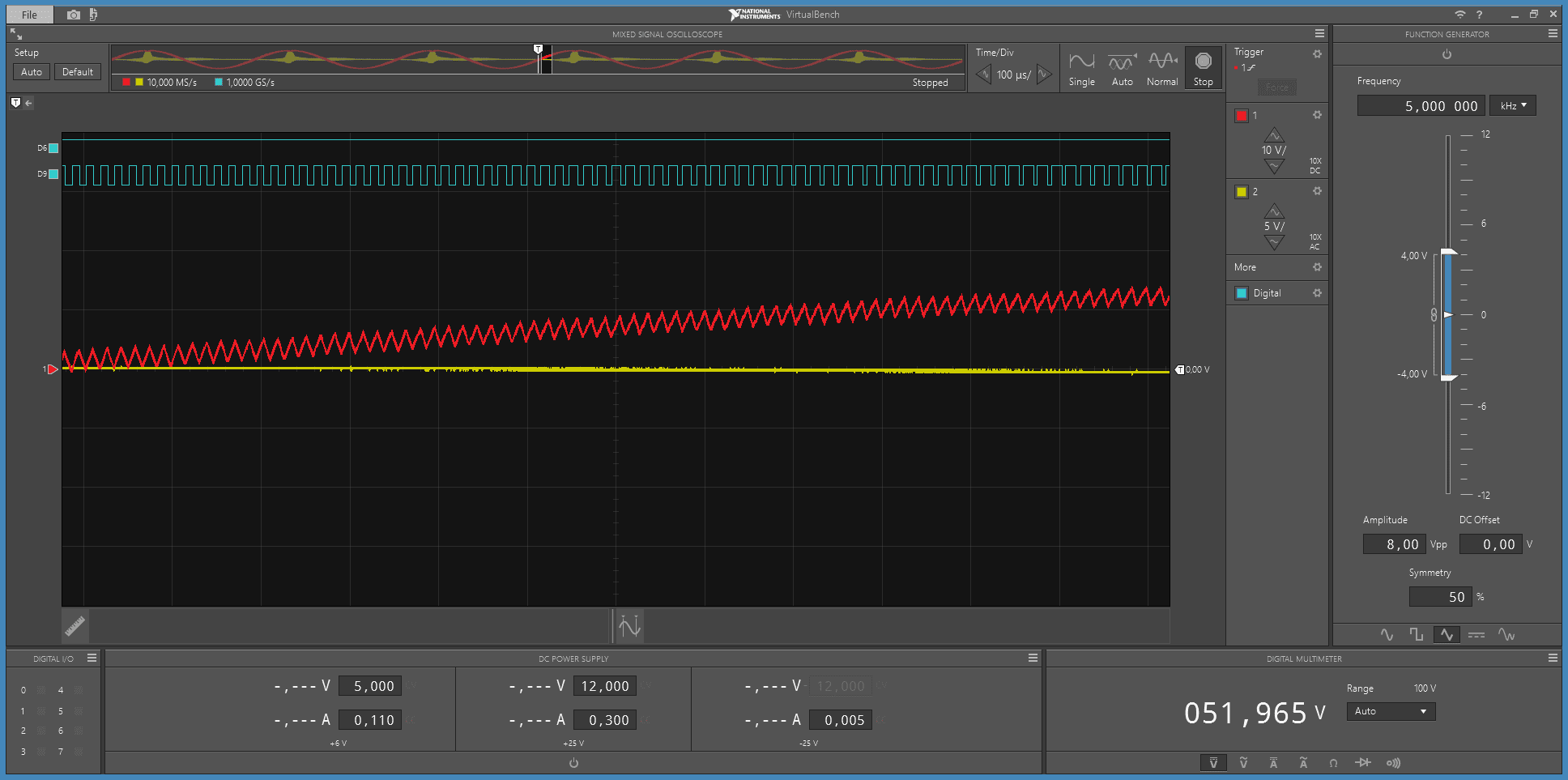
That is the Timer1 carrier surviving the single 1.2 kΩ/100 nF pole in front of the amplifier. One pole leaves a triangle of roughly 5 V × (8 µs / 120 µs) = 0.33 V p-p at the input, and ×19.3 of gain makes 3 V of it at the winding. The measurement agreed with the arithmetic to 10 %.
There was a nice confirmation of the mechanism hiding in the numbers: the residue is largest mid-slope and smallest at the crest, because a PWM triangle scales as d·(1−d) and the duty cycle approaches 100 % at the peak.
The motor could not care less — at 62.5 kHz the winding is 20 kΩ, so this drives 0.15 mA. But it costs headroom, and it puts harmonics onto 35 m of cable running up a tower next to my antennas, which is a receiver problem waiting to happen. A second identical RC pole fixed it: 47× of attenuation becomes about 2200×, at a cost of 7.7° of phase lag at 60 Hz. And because that lag is identical in both channels, the 90° quadrature between them is untouched — which is the only thing this circuit really cares about.
The sawtooth disappeared. The notch didn’t.
Suspect 3: supply noise getting in
The rail, probed at the boost converter’s output and AC coupled, turned out to be having a much more exciting time than I expected: a 15 V p-p burst of ringing, half a millisecond long, at exactly the moment of the notch.
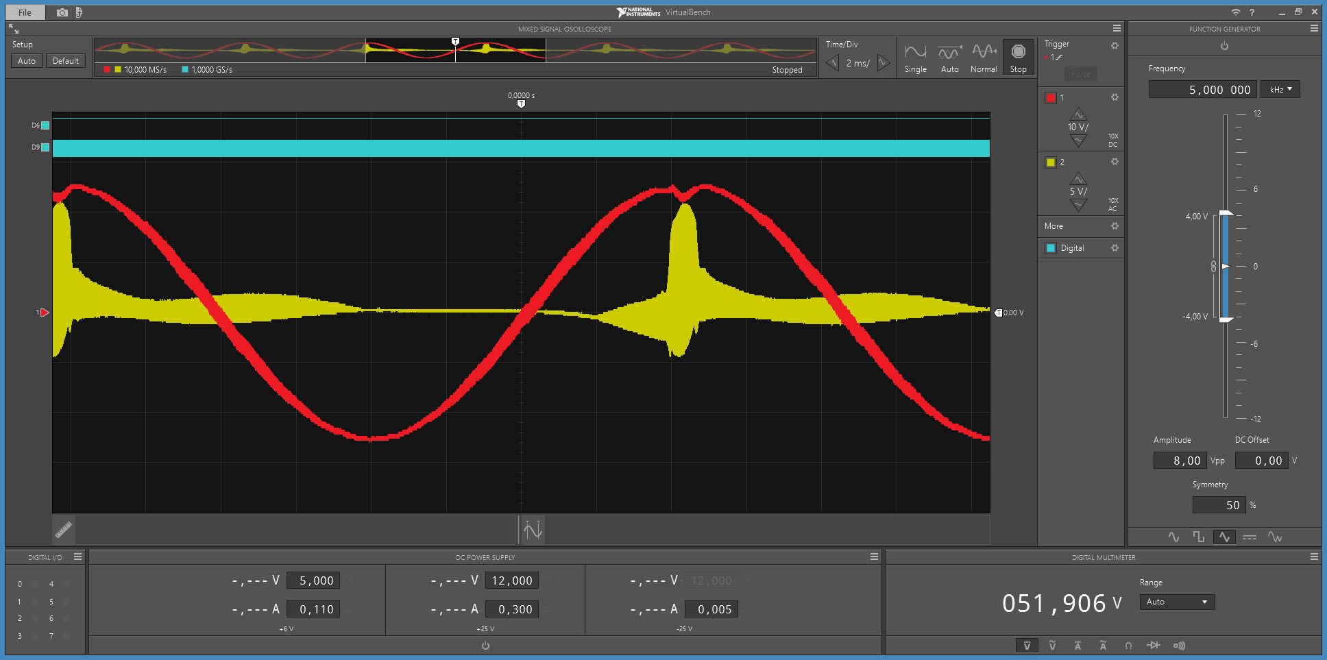
So: 15 V of rail disturbance, finite power-supply rejection, 2 V in the output. Obvious, surely. I moved the 1000 µF and 100 nF decoupling right onto pins 13/15 of the chip.
The first thing that taught me is that the burst was never a chip-side phenomenon. Measured at the supply pins it had been about 1.6 V p-p all along — 70 cm of wire and the local capacitors were already filtering it before I touched anything. Moving them onto the pins took it to 0.88 V p-p: a real improvement, and a modest one.
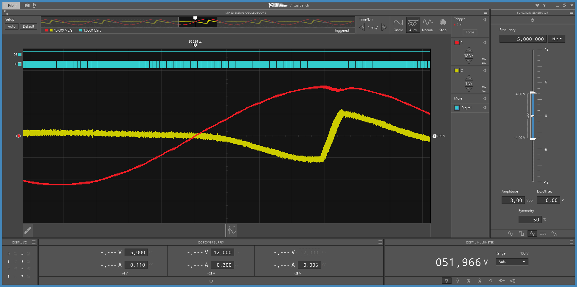
And the notch was unchanged: −1.67 V, against −1.66 V before. One variable moved, output identical. Hypothesis dead.
That negative result was the most useful measurement of the whole session.
Suspect 4: the rail sagging, and what the midpoint reference does about it
Here is the thing about a single-ended amplifier on a single supply: it draws a half-wave rectified current from the rail. The top device sources current on positive half-cycles; on negative half-cycles the current comes out of the output coupling capacitor and the rail sees nothing at all. So a 60 Hz sine into 22 Ω presents the converter with a load swinging between 0 and 1.1 A at 60 Hz, against an average of only 0.36 A.
The boost converter answered that load step the way a control loop with no bulk capacitance does: it sagged, then overshot, then rang.
Meanwhile the amplifier’s midpoint reference — the 26 V that the output swings around — is derived from the rail through a divider with a 0.5 second time constant. So it stays pinned at the average rail/2 while the instantaneous rail collapses underneath the crest.
The output was clipping into a rail that was moving.
The fix
4700 µF of low-ESR bulk directly at the boost converter’s output, so the capacitor supplies the crest and the converter only ever sees the average.
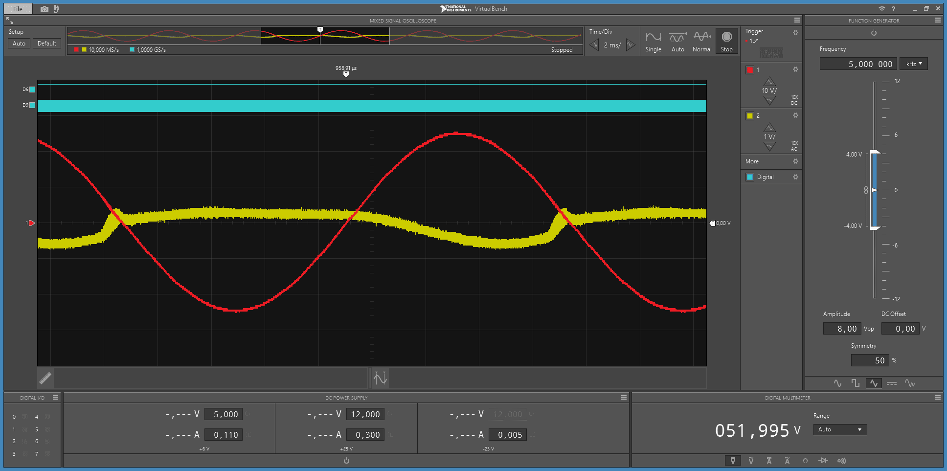
| Before | After | |
|---|---|---|
| Crest deviation from ideal sine | −1.67 V | −0.14 V |
| Total residual | 1.5 % | 0.69 % |
| Rail sag at the chip | 2.12 V p-p | 0.93 V p-p |
| Rail ripple at the chip (worst case) | 0.88 V p-p | 0.63 V p-p |
| Output | 15.9 V RMS | 17.5 V RMS |
17.5 V RMS at 60 Hz is 0.29 V/Hz, which is the design flux for this motor. The notch is gone, and with the rail behaving, the chip’s real saturation voltage finally fell out of the numbers: 0.66 V at 1.1 A — matching that 0.59 V I had measured back at the 30 V rail and not understood at the time.
Which gives a design rule for choosing the rail voltage:
V_pk ≤ rail/2 − sag − V_sat
What I would tell myself two days ago
AC-couple the scope when hunting a small feature on a big DC rail. I spent an embarrassing while trying to resolve a 1 V sag at 20 V/div, where it is 0.05 of a division and I was effectively reading trace-edge pixels. At 1 V/div AC coupled it is two divisions and unambiguous.
Probe location is part of the measurement. The same burst was 14 V p-p at the converter and 1.6 V p-p at the chip, 70 cm of wire away. Both numbers are true; only one of them is what the chip sees.
Trust negative results. Two of the four hypotheses died to a single measurement each, and the one that hurt to give up — the bootstrap, which had a beautiful mechanism and a genuine design smell behind it — was simply wrong.
Schematic symbols can lie. The 10 kΩ level trimmer was drawn as a series rheostat rather than a divider. Built that way it can only attenuate to 0.69× against the 22 kΩ bias impedance — not enough to reach the design level — and its wiper floats, leaving the input coupling capacitor charged to 26 V with nothing to discharge into except an Arduino pin. Neither problem was visible until a multimeter went on the wiper and the reading slowly decayed.
Audio values are not 5 Hz values. Every capacitor in this circuit needed rethinking for a signal that goes down to 5 Hz and sits near the rail for milliseconds at a time.
Next
Channel B — currently blocked on a 4700 µF capacitor, because the one now sitting on the converter’s output was earmarked as channel B’s output coupler. Then both channels into the real motor, where the load is inductive rather than a pair of very hot power resistors, and where the two half-wave supply demands will interleave 90° apart and hopefully treat the converter more kindly than one channel alone did.
And then, finally, the part this was all for: telling the rotator to go to 237° and watching it get there.